
Paper: GS – III, Subject: Science & Technology, Topic: S&T Initiatives – India and Global, Issue: India’s Semiconductor Vision Beyond the Shop Floor.
Context:
Recently, the Union Cabinet approved the second phase of the India Semiconductor Mission, shifting attention from factories towards an innovation ecosystem. The ₹1,27,500-crore outlay supports design, research, equipment, materials and intellectual property.
Key Takeaways:
Explanation:
Shift Towards Innovation:
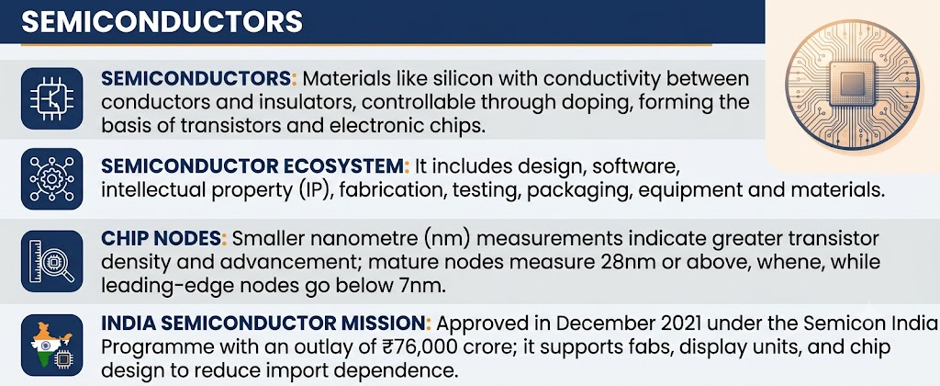
| Mature chips use older, proven technology for everyday devices, while advanced chips use newer technology for high-performance applications. |
Design priority: A 75% subsidy for semiconductor design expenditure demonstrates the importance given to Research and Development (R&D).
- Value beyond manufacturing: Countries can become semiconductor leaders by designing chips and developing software, even without manufacturing advanced chips themselves.
- Reoriented incentives: Support should promote domestic raw materials, specialty chemicals, industrial gases and equipment instead of only fabrication.
India’s Two-Level Strategy:
- Immediate opportunity: India plans to manufacture mature chips measuring 28 nanometres or above, matching current capabilities.
- Strong demand: Mature chips constitute around 70% of demand and serve smartphones, power grids and medical equipment.
- Future ambition: Developing 7-nanometre and 2-nanometre chips within five years is important, although aspirational.
Challenges:
- Geopolitical vulnerability: COVID-19 exposed shortages, while technological rivalry continues making global semiconductor value chains fragile.
- Operational requirements: Brief power cuts can destroy production; logistics, environmental approvals and regulations must remain predictable.
- Skill constraints: Manufacturing requires specialised technicians alongside engineers already working in global design companies.
Way Forward:
- Use design clusters: Centres in Bengaluru, Hyderabad, Pune and Noida should support manufacturing and innovation.
- Connect institutions: Government must enable stronger cooperation among universities, research laboratories, start-ups and industry.
- Balance support: Market competition, sustained state assistance, reliable infrastructure and skills can develop the entire value chain.
Conclusion:
Semiconductor leadership requires more than financial incentives and factories. India must convert its design talent into manufacturing strength while building research, materials, equipment and intellectual property capabilities. A complete ecosystem can deliver resilience, strategic autonomy and economic value.
Source: (The Indian Express)
La Excellence IAS Academy, the best IAS coaching in Hyderabad, known for delivering quality content and conceptual clarity for UPSC 2026 preparation.
FOLLOW US ON:
◉ YouTube : https://www.youtube.com/@CivilsPrepTeam
◉ Facebook: https://www.facebook.com/LaExcellenceIAS
◉ Instagram: https://www.instagram.com/laexcellenceiasacademy/
GET IN TOUCH:
Contact us at info@laex.in, https://laex.in/contact-us/
or Call us @ +91 9052 29 2929, +91 9052 99 2929, +91 9154 24 2140
OUR BRANCHES:
Head Office: H No: 1-10-225A, Beside AEVA Fertility Center, Ashok Nagar Extension, VV Giri Nagar, Ashok Nagar, Hyderabad, 500020
Madhapur: Flat no: 301, survey no 58-60, Guttala begumpet Madhapur metro pillar: 1524, Rangareddy Hyderabad, Telangana 500081
Bangalore: Plot No: 99, 2nd floor, 80 Feet Road, Beside Poorvika Mobiles, Chandra Layout, Attiguppe, Near Vijaya Nagara, Bengaluru, 560040