
Paper: GS-III, Subject: Science & Technology, Topic: Indigenization and Development of Technologies, Issue: India’s Complete Semiconductor Ecosystem
Context
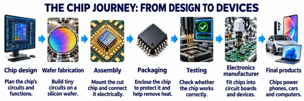
The fifth edition of SEMICON India 2026, being held at Yashobhoomi, New Delhi, from 17–19 September 2026 under the theme “Silicon to Systems: Building the Ecosystem”, is showcasing India’s transition from electronics assembly towards a complete semiconductor ecosystem. The event highlights the shift from Semicon 1.0 to Semicon 2.0, with greater emphasis on domestic design, fabrication, materials, equipment, advanced packaging, research and skilled manpower.
Background
- India’s electronics push: The National Policy on Electronics, 2019 provided the broad framework, followed by the PLI Scheme for Large-Scale Electronics Manufacturing, SPECS and EMC 2.0, which promoted electronics production, component manufacturing and industrial infrastructure.
- Semicon India 1.0: Launched in 2021, it supported semiconductor fabrication plants (fabs), display fabrication plants (display fabs), compound semiconductor manufacturing facilities, Assembly, Testing, Marking and Packaging (ATMP) units, and Outsourced Semiconductor Assembly and Test (OSAT) facilities., while the Design Linked Incentive (DLI) promoted Indian chip-design companies.
- Talent development: The Chips to Startup (C2S) programme focused on developing semiconductor design and manufacturing skills, while PLI 2.0 for IT Hardware encouraged domestic production of laptops, servers and other electronics that create demand for chips.
- Increasing domestic value addition: The Electronics Components Manufacturing Scheme and Mobile Phone Manufacturing Scheme, 2026 seek to reduce dependence on imported components and increase the share of value created within India.
- Semicon 2.0: Approved in July 2026 with an outlay of ₹1,27,500 crore, it shifts the focus from establishing individual semiconductor plants to developing the complete ecosystem required to sustain them.
Why Does India Need Semicon 2.0?
1. Reducing External Dependence
- India’s electronics market is expanding rapidly, but many critical chips, manufacturing inputs, chemicals and specialised technologies still come from abroad, making domestic industries vulnerable to global supply disruptions and geopolitical tensions.
2. Increasing Domestic Value Addition
- Manufacturing a phone, computer or vehicle in India creates limited domestic value if the processor, memory, sensors, display components and other advanced parts are imported, so the next stage of policy aims to capture more high-value activities within India.
3. Strengthening Strategic Security
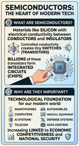
- Semiconductors are essential for defence systems, satellites, telecom networks, power infrastructure, artificial intelligence, automobiles and industrial machinery, so dependable access to chips has become an issue of both economic and national security.
What Does Semicon 2.0 Focus On?
1. Design and Indian Intellectual Property
- The programme seeks to support Indian firms and start-ups in creating their own chip designs and intellectual property so that India moves from mainly providing engineering services to also owning valuable semiconductor technologies.
2. Machines, Materials and Inputs
- Support will extend to semiconductor equipment, silicon wafers, specialty gases, chemicals and advanced materials, because a domestic fab cannot become truly resilient if most of the critical inputs required to operate it are imported.
3. More Fabrication Capacity
- India plans to expand silicon fabs as well as specialised semiconductor facilities, including compound and discrete semiconductors, so that more stages of actual chip manufacturing take place within the country.
4. Advanced Packaging
- India will strengthen ATMP/OSAT and advanced packaging capabilities, which are becoming increasingly important as multiple specialised chip components are combined into high-performance systems.
5. Research and Development
- Semicon 2.0 aims to support research in advanced semiconductor technologies, new materials, manufacturing processes and future chip architectures so that India gradually develops indigenous technological capability.
6. Talent Development
- The strategy also focuses on training engineers and technicians in areas such as VLSI design, semiconductor physics, process engineering, materials, fabrication, packaging and testing, ensuring that physical factories are supported by a skilled domestic workforce.
Progress So Far
- Under Semicon 1.0, 12 semiconductor manufacturing units with proposed investment exceeding ₹1.64 lakh crore have been approved, while domestic chip-design projects, access to advanced design tools and training initiatives have also expanded.
Conclusion
India’s semiconductor policy is now moving from “assemble electronics in India” to “build the ecosystem behind electronics in India.” Semicon 2.0 therefore seeks to deepen domestic capability across design, manufacturing, materials, research, packaging and skills while integrating India more strongly into global semiconductor supply chains.
Source: (PIB)
La Excellence IAS Academy, the best IAS coaching in Hyderabad, known for delivering quality content and conceptual clarity for UPSC 2026 preparation.
FOLLOW US ON:
◉ YouTube : https://www.youtube.com/@CivilsPrepTeam
◉ Facebook: https://www.facebook.com/LaExcellenceIAS
◉ Instagram: https://www.instagram.com/laexcellenceiasacademy/
GET IN TOUCH:
Contact us at info@laex.in, https://laex.in/contact-us/
or Call us @ +91 9052 29 2929, +91 9052 99 2929, +91 9154 24 2140
OUR BRANCHES:
Head Office: H No: 1-10-225A, Beside AEVA Fertility Center, Ashok Nagar Extension, VV Giri Nagar, Ashok Nagar, Hyderabad, 500020
Madhapur: Flat no: 301, survey no 58-60, Guttala begumpet Madhapur metro pillar: 1524, Rangareddy Hyderabad, Telangana 500081
Bangalore: Plot No: 99, 2nd floor, 80 Feet Road, Beside Poorvika Mobiles, Chandra Layout, Attiguppe, Near Vijaya Nagara, Bengaluru, 560040